Equipment:
Scanning Probe Microscope NT-MDT NTegra Aura
- Atomic Force Microscopy
- Phase Imaging
- Electrostatic Force Microscopy
- Kelvin Probe Force Microscopy
- Magnetic Force Microscopy
- Scanning Spreading Resistance Microscopy
- Scanning Tunneling Microscopy
- Nanolithography (Local Anodic Oxidation and Scratching)
- Tunneling spectroscopy and electrical transport measurements
- Active anti-vibration table
- Measurement in controlled environment (various gases) or vacuum
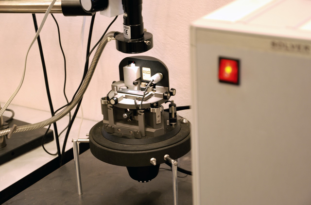
Scanning Probe Microscope NT-MDT Solver P47 Pro
- Atomic Force Microscopy
- Phase Imaging
- Electrostatic Force Microscopy
- Kelvin Probe Force Microscopy
- Magnetic Force Microscopy
- Scanning Spreading Resistance Microscopy
- Scanning Tunneling Microscopy
- Nanolithography (Local Anodic Oxidation and Scratching)
- Tunneling spectroscopy and electrical transport measurements
- Humidity control
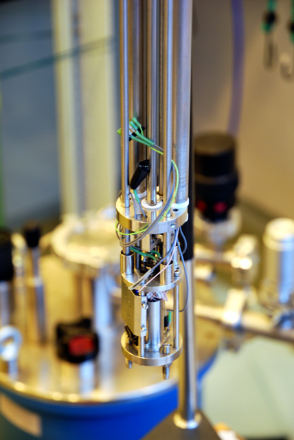
Cryogenic Scanning Tunneling Microscope NT-MDT
- Scanning Tunneling Microscopy
- Local Tunneling Spectroscopy and Transport Measurements
- operating temperature range 1,5 – 300 K
Oxford Instruments Optibath SXM Cryostat
operating temperature range 1,5 – 300 K
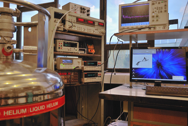
Transport Measurements Setup
- 2x LHe inset
- Keithley 220 Current Source
- 2x Keithley 2000 Multimeter
- Stanford Research Systems SR830 DSP Lock-In Amplifier
- Operating temperature range 4,2 – 300 K
- I-V, R-T, Ic-T and dI/dV-V characteristics
- Tunneling spectroscopy
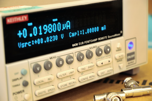
Low Current / High Resistance Measurements Setup
- Keithley 6430 Sub-Femtoamp Remote SourceMeter
- HP 34401A Multimeter
- LHe inset
- Operating temperature range 4,2 – 300 K
- I-V and R-T characteristics (current measurement with sub-femtoamp resolution, resistance measurement up to 20 TOhm)
Typical results:
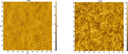
AFM topography of poly-crystalline TiO2 thin film (left) and nano-crystalline TiB2 thin film (right) deposited by magnetron sputtering.
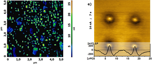
Scanning Spreading Resistance Microscopy image of YBCO surface (left) and Kelvin Probe Force Microscopy image of surface potential patterns created on hydroxyapatite films by focused electron beam.
![]()
Typical current-voltage characteristics of YBa2Cu3O7-x/Ag planar junctions exhibiting resistance switching behavior (left) and differential (dI/dV-V) characteristics of point-contact junction on MgB2.
Staff:
RNDr. Tomáš Plecenik, PhD.
e-mail: tomas.plecenik@fmph.uniba.sk, Phone: +421-2-60295-274, 243, 190
Ing. Maroš Gregor, PhD., Prof. RNDr. Andrej Plecenik, DrSc., Prof. RNDr. Peter Kúš, DrSc.
PhD. Students:
RNDr. Martin Truchlý
e-mail: martin.truchly@fmph.uniba.sk, Mobile phone:
Mgr. Robert Sobota:
e-mail: robert.sobota@fmph.uniba.sk, Mobile phone:+421 915 474 352